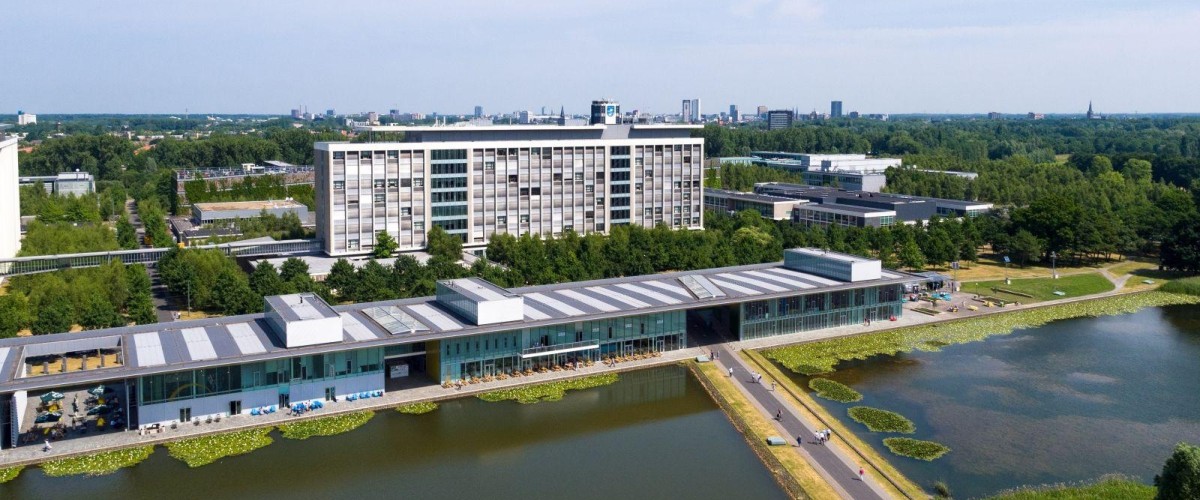
Once a printing company, now a high-tech conglomerate with 37,000 employees worldwide. Starting in September, the High Tech Campus Eindhoven will welcome Dai Nippon Printing (DNP) from Japan, following initial contact in 2023. The Brabant Development Agency (BOM) played a key role in this process, bringing this global leader in precision coating technology, among other things, to Brabant.
It all started in November 2023 during the Brabant Innovation Days in Tokyo, says Edwin Zonder of BOM. There he met Tsuyoshi Hotta. “And Hotta-san was very interested in Brabant because of our high-tech ecosystem.”
That meeting was no coincidence, Zonder quickly realized. “He wanted to speak to me right away and even take a picture with me,” Zonder laughs. “The meeting was arranged by the Netherlands Foreign Investment Agency in Japan. They knew Hotta-san had his eye on the High Tech Campus and wanted to know more about the ecosystem.”
Why? “Because Brabant offers a unique network of knowledge institutions, companies, and facilities that is recognized all over the world,” says Hotta-san, who focuses on partnerships outside Japan on behalf of DNP. “For DNP, it’s the ideal place to develop new technology and work with partners who are global leaders in photonics and semicon.”
Fact finding trip
That first meeting in 2023 was the starting signal for Zonder to take action. As Senior Project Manager Foreign Investments at BOM, he and his colleagues look at foreign companies that could potentially strengthen existing Brabant value chains. And he maintains a broad and specialized network within Brabant. Zonder: “We immediately got to work telling DNP all about Brabant and showing them around.”
A few months later, in July 2024, a Japanese delegation led by Hotta-san visited. “A so-called fact-finding trip, so they could see what Brabant has to offer and how things work here.”
BOM organized the trip. “We know our way around Brabant very well,” says Zonder. “We seated them with people who could be relevant to them, potential collaboration partners. We told them about Japanese companies already established here, and about the high-tech ecosystems in Brabant and the rest of the Netherlands. We really rolled out the red carpet for them.”
Holst Centre as a partner
In the months that followed, contact remained close between Zonder, the Netherlands Foreign Investment Agency, and Hotta-san. Eventually, Holst Centre emerged as a potential partner. Founded in 2005, Holst Centre is a joint research center of Imec (Leuven) and TNO. “In November 2024, DNP wanted to see some of Holst Centre’s labs,” says Zonder. “They asked for very specific information about the facilities.” DNP will now partly use those facilities.
“We saw the clean room laboratory facilities at the High Tech Campus and TU/e and got a real sense of the affinity with DNP's technology”, says Koichi Suzuki, who will become the Director of the DNP's new Research base in Eindhoven. “As the saying goes, ‘seeing is believing’.”
“The combination of TNO’s experience in applied research and system integration with our expertise in microfabrication and precision coating is extremely valuable for us,” says Hotta-san. “Holst Centre offers the infrastructure and network we need.”
DNP and TNO are starting a joint research and development hub at Holst Centre. They will work together with the Photonic Integration Technology Centre (PITC) on a three-year program. DNP is aiming for a long term relationship with Brabant. This is the first time in DNP’s long history—founded in 1876—that the company is establishing an R&D hub outside Japan.
“The fact that more and more Japanese companies are setting up R&D facilities in Brabant is a huge step. For companies like this, it’s really not self-evident,” says Zonder. “We benefit greatly from DNP coming to Eindhoven. It’s an incredibly important player for our entire ecosystem around semicon and photonics.”
Co-Packaged Optics: bridging light and electronics
The collaboration focuses on developing Co-Packaged Optics, an essential technology for the next generation of computer chips. Here’s how it works.
Every year, we send more and more data. Think of video calling, online shopping, streaming movies, and using artificial intelligence. Data centers process all that information at lightning speed. This consumes a lot of energy. That’s why companies and scientists are constantly looking for ways to transmit data more efficiently.
A smart solution is photonics: sending data via light signals. This principle is already familiar from fiber optic networks, which can transmit huge amounts of information quickly and energy-efficiently. But ultimately, that information must be converted back into electronic signals so computers can process it.
All in one
That’s where Co-Packaged Optics comes in. This technology integrates optical and electronic components into a single system, such as a chip. This allows signals to be converted from electricity to light and back again faster. It also reduces energy loss, improves data center performance, and lowers power consumption.
“Normally, optical components like lasers are separate from the electronic ones, for example in a separate module connected by cables,” explains Toine Cleophas, Senior Project Manager High Tech at BOM. “With Co-Packaged Optics, the optical components are placed directly next to, or even on the same chip as, the electronic ones.”
The result? Light signals have less distance to travel between the optics and the processor. This means less latency and higher speeds. Cleophas: “Moreover, converting signals consumes energy. The shorter the distance, the less energy it costs. And electronic components generate heat. By smartly integrating optical components, you can manage that heat better and save energy.”
With this collaboration, the already growing photonics industry in Southeast Brabant gains a major international player. A partner who not only brings technology, but also new opportunities for collaboration, innovation, and economic growth in the region.

Find out more?

Edwin Zonder

